
Study on Nanostructures and Charge Transport Properties of Arrayed Inorganic Semiconductors in Suzhou Nanotechnology Institute
Inorganic semiconductor nanostructured electrodes have a very wide range of applications in solar cells, photolysis water, and energy storage devices. The specific surface area of ​​the electrodes and the charge transport capability are the key factors that determine the performance of these devices. Recently, researcher Feng Xinjian of the Institute of Nanotechnology and Nano-Bionics of the Chinese Academy of Sciences has made a series of new developments in the research of high-performance inorganic semiconductor nano-electrodes.
The microstructure of the electrode material has an important influence on its electrical properties. The traditional electrode material with high specific surface area is formed by disorderly packing of nanoparticles. Due to the presence of a large number of grain boundaries and defects between crystal grains, the diffusion constant of charges in the crystal is lower than that in single crystal bulk materials. -8 orders of magnitude, seriously affecting the performance of the device. One-dimensional nanostructured array electrodes provide direct channels for charge transport. In the previous work, relevant persons successfully prepared a one-dimensional array of one-dimensional TiO2 nanowires on a transparent conductive glass by solvothermal method, and proved that the structure has 200 times faster electron transfer rate than the nanoparticle film by transient photoelectric test methods. (Angew. Chem. Int. Ed. 2012, 51, 2727–2730). By using the array structure electrode in a perovskite solid-state solar cell, a photoelectric conversion efficiency of nearly 12% was achieved (Chem. Comm. 2014, 50, 14720-14723. inner cover).
Array one-dimensional nanostructures possess rapid charge transport properties, but their specific surface area is much smaller than that of nanoparticle films. Therefore, nanostructures with high specific surface area and rapid charge transport properties are prepared by rationally regulating the microstructure of the electrodes. It is an important direction for the development of inorganic semiconductor nano-electrode materials in the future. Recently, researchers have prepared electrode materials that have both a high specific surface area and fast charge transport properties through two ways of regulating the microstructure.
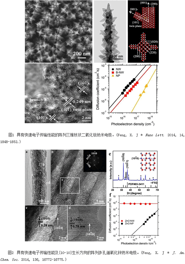
First, an array of three-dimensional branched electrode structures was prepared on the basis of an array of one-dimensional TiO2 nanowires. The branched structure is epitaxially grown along a one-dimensional trunk, which greatly reduces grain boundaries and defects between the branches and the trunk. The electrode structure has similar fast electron transport properties to the one-dimensional structure of the array, but its specific surface area is increased by 71% over the one-dimensional structure and brings about 52% improvement in the photoelectric conversion rate. Relevant work was published in Nano Lett. 2014, 14, 1848-1852, and received extensive attention, becoming the top 20 articles in the magazine with the most monthly readings.
Second, a single crystal-like array porous structure was prepared by lattice contraction of a large lattice material. By modulating the coordination dynamic process of metal ions, an array of single-crystal one-dimensional hydroxyfluoride zinc nanomaterials with a large lattice was prepared. Based on this, controllable processing was carried out, and along with the directional shrinkage of the unit cell of zinc hydroxyfluoride and the removal of small molecules, an array of porous zinc oxide nanowires with single crystal properties was obtained for the first time. This transformation also allows the prepared arrayed zinc oxide nanowires to have a special [10-10] lattice orientation. The electrode material with a thickness of 25 microns has a surface roughness factor of 955, which is comparable to a conventional nanoparticle film, and its electron transport speed is at least 1000 times faster than the nanoparticle film, and it is an ideal electrode structure. Related work was published in J. Am. Chem. Soc. 2014, 136, 16772-16775.
The above research work has received extensive attention from international counterparts. At the invitation of SPIE, he wrote a synthesis and assembly of 1D semiconductor for solar energy conversion and published it on SPIE's official website.
This series of work was supported by the national youth thousands plan, the National Natural Science Foundation of China, the Chinese Academy of Sciences and the Suzhou Nano Institute.
SIC
Emery, also known as Silicon Carbide (SiC), is produced by high-temperature smelting of resistance furnaces using quartz sand, petroleum coke (or coal coke), and sawdust (need to add salt when green silicon carbide is produced). Silicon carbide also has a rare mineral, Moissanite, in nature. Silicon carbide is also called Carbon silica. Among the non-oxide high-tech refractory raw materials such as C, N, B, etc., silicon carbide is the most widely used and the most economical one, and it can be called gold grit or refractory sand. At present, China's industrial production of silicon carbide is divided into two types of Black Silicon Carbide and green silicon carbide, are hexagonal crystals, the specific gravity of 3.20 ~ 3.25, the microhardness of 2840 ~ 3320kg/mm2.
Silicon carbide has two common basic varieties of black silicon carbide and green silicon carbide, both of which are α-SiC. 1 Black silicon carbide contains about 95% of SiC. Its toughness is higher than that of green silicon carbide. It is mostly used for processing low tensile strength materials such as glass, ceramics, stone, refractory materials, cast iron and non-ferrous metals. 2 Green silicon carbide contains more than 97% SiC, self-sharpening, mostly used for processing hard alloys, titanium alloys and optical glass, also used for honing cylinder liners and grinding high-speed steel cutters. In addition, there is cubic silicon carbide, which is a yellow-green crystal made by a special process, used for the production of abrasives for bearing superfinishing, surface roughness can be processed from Ra32 ~ 0.16 microns to Ra0.04 ~ 0.02 micron.
Silicon Carbide
Silicon Carbide,Black Silicon Carbide,Silicon Carbide For Abrasives,High Purity Silicon Carbide
Hwa Seng Resources (Hong Kong) Co., Limited , https://www.hwaseng-resources.com