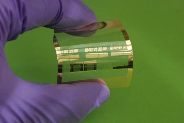
New Breakthrough in MOSFET Technology: High Performance Transistor Surface Based on Flexible Plastic Film
According to foreign media reports, UW Madison researchers at the University of Wisconsin have teamed up with partners to achieve a breakthrough approach. This not only greatly simplifies the manufacturing process for low-cost, high-performance, wirelessly flexible metal-oxide-semiconductor field-effect transistors (MOSFETs), but it also overcomes many of the operational problems encountered when using standard technologies for manufacturing equipment. This technology can be used to manufacture large rolls of flexible plastic printed circuit boards, and is used in fields such as wearable electronic devices and bend sensors.

The researchers said that this breakthrough nanoimprint lithography manufacturing process can create a complete roll of very high performance transistors on ordinary plastic sheets.
Due to the excellent low current demand and better high frequency performance, MOSFETs have rapidly replaced common bipolar transistors in electronic circuits. In order to meet the ever-shrinking demand for integrated circuits, the size of MOSFETs is also becoming smaller, but this has also caused some problems.
Specifically, the MOSFETs can effectively generate current flow because standard semiconductor fabrication techniques cannot precisely control the level of doping (doped in silicon to bring either positive or negative charge) to ensure cross-component Consistency of channel performance.
The MOSFET is usually formed on a silicon dioxide (SiO2) substrate and then deposited with a layer of metal or polysilicon. However, this method can be inaccurate and difficult to control completely. Doping sometimes leaks out to other places that are not needed. This creates a so-called “short-channel effect†area and leads to a decrease in performance.

A cross section of a typical MOSFET at different levels.
However, the University of Wisconsin-Madison has teamed up with multiple partners across the United States (including the University of Michigan, the University of Texas, and the University of California, Berkeley) to develop new technologies that reduce dopant leakage to improve semiconductor quality. Researchers create custom shapes and shapes on the surface through electron-beam lithography, resulting in a more "physically controllable" production process.
In summary: (1) The research team started with 'positive doping' of a 270-nm-thick silicon surface coating, followed by electron-beam lithography to create nano-trenches, followed by dry etching to prepare silicon nano-films. (2) Subsequently, the researchers took out the silicon nanofilm layer and moved it to another substrate film coated with adhesive plastic. (3) The last step is to add an additional demulsifier to isolate and define the channel region and deploy the gate dielectric layer and the metal gate.
Although it sounds a lot of work, it is a relatively simple process compared to current semiconductor manufacturing processes. In fact, it has been reported that a new type of transistor is operating at a record-breaking speed of 38 GHz. Simulations show that it can even reach 110 GHz after a slight optimization.
In addition to the speed increase, the new technology has not affected the further reduction of the process. Researchers also claim that the new transistor is particularly suitable for radio frequency applications because it is designed for wireless data transmission and power, and wearable electronics and sensors will prove to be of great value.
The details of the current study have been published in the recently published "Scientific Reports" journal.
Glucose Test Drink,Sodium Gluconate In Food,Sodium Gluconate Uses In Cosmetics,Sodium Gluconate Chelating Agent
Shaanxi United Xingchuang International Co., Ltd. , https://www.lxcgj.com
