
The Institute of Chemistry has made progress in printing and preparing multilayer embedded flexible circuits
Because of the advantages of environmental protection, low cost, and flexibility, flexible printed circuits are expected to replace traditional electronic devices based on lithography. Inkjet printing technology can directly realize the patterning of metal nanoparticles, and is one of the most promising methods for preparing nano-printed electronic devices. However, inkjet printing technology has limited its application in the field of high-precision, highly-integrated circuit preparation due to difficulties such as spreading and fusion of ink droplets.
Under the strong support of the National Natural Science Foundation of China, the Ministry of Science and Technology, and the Chinese Academy of Sciences, researchers at the Green Printing Key Laboratory of the Institute of Chemistry, Chinese Academy of Sciences have systematically researched the interaction between the ink droplets and the substrate by controlling the ink droplets at the base. The infiltration behavior of the material surface has led to a series of extensive and in-depth studies in controllable high-precision printing and printing technology (Adv. Mater. 2014, 26, 6950-6958). By controlling the properties of inks, substrates and other materials, they successfully prepared a series of high-precision patterns: using the “coffee ring†phenomenon to produce high-precision conductive patterns of metallic nanoparticles with line widths up to 5 μm (Adv. Mater. 2013, 25, 6714-6718); Print high-precision three-dimensional functional patterns using the three-phase line-slip phenomenon of printing ink drops (Adv. Opt. Mater. 2014, 2, 34-38; Adv. Funct. Mater. 2015, 25, 2237 -2242); A series of special three-dimensional columnar structures with controllable shape have been prepared by the magnetic field-induced three-phase line dynamic retraction (Small 2015, 11, 1900-1904); high precision has been achieved by "ink-jet imprinting" using soft substrates. The micro-pit and groove structure (Adv. Funct. Mater. 2015, 25, 3286-3294); The conductive pattern with an accuracy of 30 nm was prepared by controlling the nano-materials on the printed electrode template with controllable assembly printing (Adv. Mater. 2015, 27, 3928-3933). They used these printed, printed functional patterns to achieve plasma lightwave transmission (Adv. Mater. 2014, 26, 2501-2507) and high sensitivity detection (Angew. Chem. Int. Ed. 2014, 53, 5791-5795; Nanoscale 2015, 7, 421-425), Quantum Dot Patterns (Small 2015, 11, 1649-1654), Biological Cell Separation (ACS Appl. Mat. Interfaces 2015, 7, 9060-9065), Lab on a Chip 2015, 7, 1759-64) and high-precision flexible circuit preparation (Adv. Mater. 2015, 27, 3928-3933) and other applications.
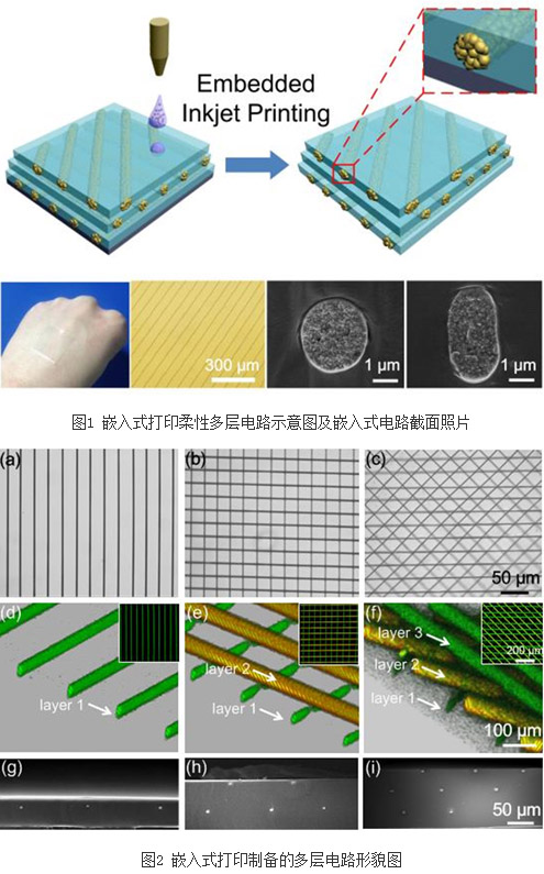
Based on the above research, they used a conductive ink containing nanoparticles on a polymerizable liquid substrate to subtly utilize the dynamic enveloping effect of the liquid substrate on the printing ink droplets, thereby realizing the direct preparation of high-precision embedded conductive silver wires. . Due to the influence of viscosity and surface tension of the ink-jet printing conductive ink, it is very challenging to realize that it is fused into a line inside another liquid. They solved this problem by regulating the rheological behavior of the liquid substrate and the properties of the nanosilver conductive ink, enabling controllable encapsulation of droplets by liquid substrates, effectively suppressing the diffusion of ink droplets and the effect of "coffee rings" ( figure 1). Based on this, a conductive silver wire with a line width of about 1-2 μm was fabricated using an ordinary commercial printer with an aperture of 25 μm, which is approximately 20 times more accurate than usual ink-jet printing. The prepared high-precision circuit is embedded directly inside the substrate, avoiding subsequent packaging steps. Electrical tests show that the embedded micro-cable prepared by this method has excellent electrical conductivity. They further used this “liquid film embedded printing†to directly print and realize the preparation of multi-layer circuits by layer-by-layer stacking, achieving the integration of three-layer circuits embedded in 60 μm transparent films (Figure 2).
The "liquid film embedded printing" in this work is a universal method and is also applicable to conductive materials such as carbon nanotubes, graphene, and the like. It is of great significance to improve the precision and integration of the printing circuit and to prepare ultra-high transparent embedded electronic devices, and lays a technical foundation for printing and preparing high-integration, high-precision three-dimensional structural circuits. The research results were published on the recently published Adv. Mater. 2016, 28, 1420–1426.
stainless steel sink strainer can be used for fruit and vegetable washing drain basket, it is a useful stainless steel kitchen tool and it also called Draining Rack or draining basket. It is very useful when you wash your fruit and vegetable, it will make your fruit and vegetable health to eat.
The material is food grade 304 stainless steel which is anti rust and easy to wash
Fruit Vegetable Washing Draining Basket,Stainless Steel Kitchen Tool,Draining Rack, Draining Basket
Shenzhen Lanejoy Technology Co.,LTD , https://www.brassinsert.net